
Telecom hardware is where dimensional accuracy stops being a nice-to-have. An optical module shell has to locate a transceiver to a few hundredths of a millimetre while also acting as a heat path and an EMI shield, and a 5G radio unit has to survive years on a mast. These are the parts where our tolerance capability matters most, and where the difference between a supplier who owns the process and one who brokers it shows up in field failure rates.
What makes this enclosure difficult
These are the failure modes we see most often in this application — and the ones we design against from the first section drawing:
- Optical alignment tolerance. The bore that locates the transceiver port cannot drift, or insertion loss and return loss move with it.
- EMI shielding has to be continuous. Anodising is an insulator, so the grounding and shielding strategy has to be designed into the surface treatment and the joint design together.
- Thermal load in a shrinking envelope. 800G modules dissipate more heat in a smaller cage than the generation before.
- Volume consistency. Telecom customers qualify a part once and then buy it for years — the ten-thousandth unit has to match the first.
How we handle it
±0.04 mm bores held in volume
Our internal standard for inner and outer diameter is ±0.04 mm against a GB standard of ±0.10 mm. For optical module cages and transceiver shells this is the dimension that protects your insertion-loss budget, and we hold it across the run rather than on first articles only.
0.3 mm fins inside the module envelope
Where the shell also has to dissipate heat, we extrude fins as thin as 0.3 mm into the section so the cooling area grows without growing the module footprint.
EMI considered before the finish is chosen
Standard anodising insulates. If you need a conductive surface we discuss conductive oxidation, selective masking of grounding faces, or nickel plating, and design the joint so the shield path is continuous. Tell us the requirement at enquiry stage and we build it into the process route.
Free DFM review before the die is cut
Our engineers check wall uniformity, corner radii, bore feasibility and shielding continuity on your 3D model and come back within one working day. Most telecommunication enclosures get at least one geometry suggestion at this stage, and every one of them is free.
Machined features in one setup
Connector windows, threaded holes, grounding pads and datum faces are machined in the same fixturing, so positional relationships hold rather than accumulating across operations.
Capability that matters here
| Parameter | Typical capability | Why it matters |
|---|---|---|
| Inner / outer diameter tolerance | ±0.04 mm | Protects optical alignment and insertion loss |
| Wall thickness tolerance | ±0.02 mm | Consistent shielding and stiffness |
| Minimum fin thickness | 0.3 mm | Cooling area inside a fixed envelope |
| Cut-to-length accuracy | ±0.005 mm | Repeatable cage assembly |
| Datum face machining | Same setup as other features | No tolerance stack-up across operations |
| Shielding finishes | Conductive oxidation, selective masking, nickel plating | Continuous EMI path where required |
Typical parts we make for this industry
- 400G / 800G optical transceiver module shells
- 5G AAU and RRU heat sink enclosures
- Baseband unit and small-cell housings
- Fibre distribution and splice enclosure bodies
- Base station power supply cases
- Optical test instrument chassis
Material and finish
6063-T5 is standard for optical and RF housings because it extrudes to fine detail and gives a stable, uniform anodised layer. 6061-T6 is used where the part also serves as a structural bracket or carries tapped holes under load.
Our polish-free 6063 route runs primary billet from a state-owned mill through ceramic filtration, degassing and homogenising, so the profile goes straight to 180# blasting and anodising with no polishing stage — typically around 15% less finishing cost. We deliberately do not take high-pressure die-casting work; all capacity goes into extruded profile and precision machining.
Questions buyers in this industry ask
Anodising insulates — how do you handle EMI shielding?
By deciding before production, not after. Options include conductive oxidation instead of standard anodising, masking the grounding faces so they stay bare metal, or nickel plating. Which one is right depends on your grounding strategy and shielding target, so we discuss it during DFM review and write it into the process route.
Can you hold optical alignment tolerances across a full production run?
Yes, and we supply dimensional reports on request so you can verify it rather than take our word. Our internal diameter standard is ±0.04 mm; the die defines the section and we check in-process, so drift is caught during the run rather than at final QC.
We are still qualifying — can we get prototypes before committing to tooling?
Yes. We can machine prototype quantities from solid bar so you can complete optical and thermal validation without opening a die. That costs more per piece but removes tooling risk, and most telecom customers start exactly this way before moving to extrusion.
Where we ship these
Other industries we serve
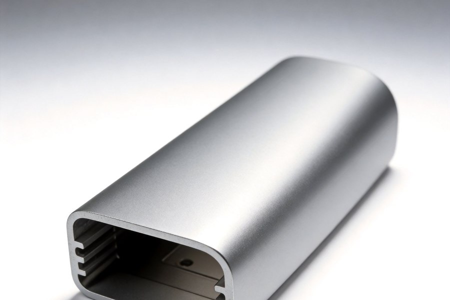
Heat Sink & Thermal Enclosures
Extruded aluminium heat sink enclosures with 0.3 mm fins, machined mounting faces at 0.05 mm flatness and polish-free 6063…
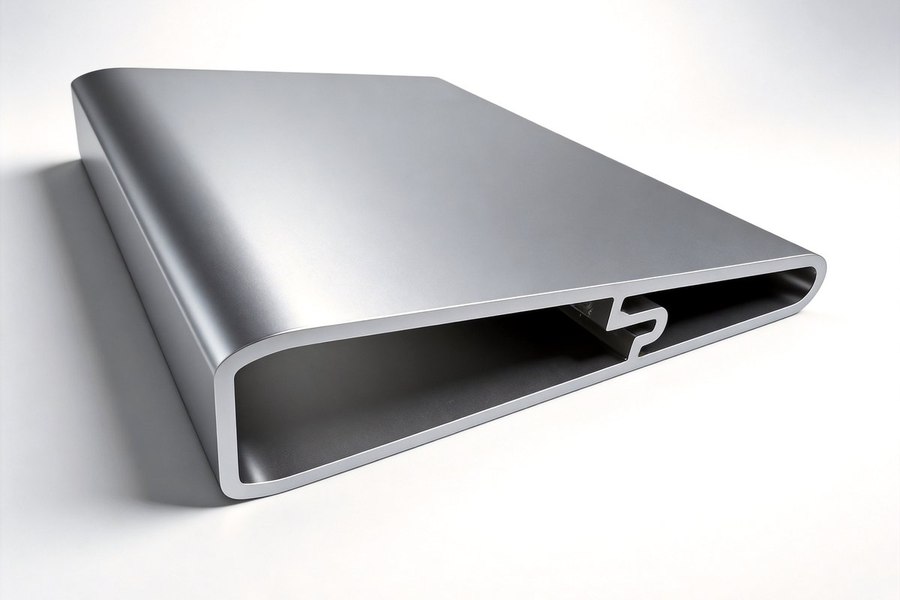
Energy Storage & Battery Enclosures
Extruded aluminium enclosures for portable power stations, home storage modules and BMS control boxes — 0.5–2.0 mm walls, ±0.005…
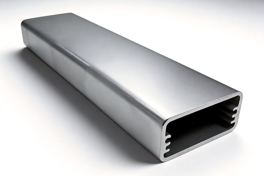
Automotive Electronics Enclosures
Vibration and temperature-cycled aluminium housings for on-board chargers, ECUs, display frames and auxiliary lighting —…
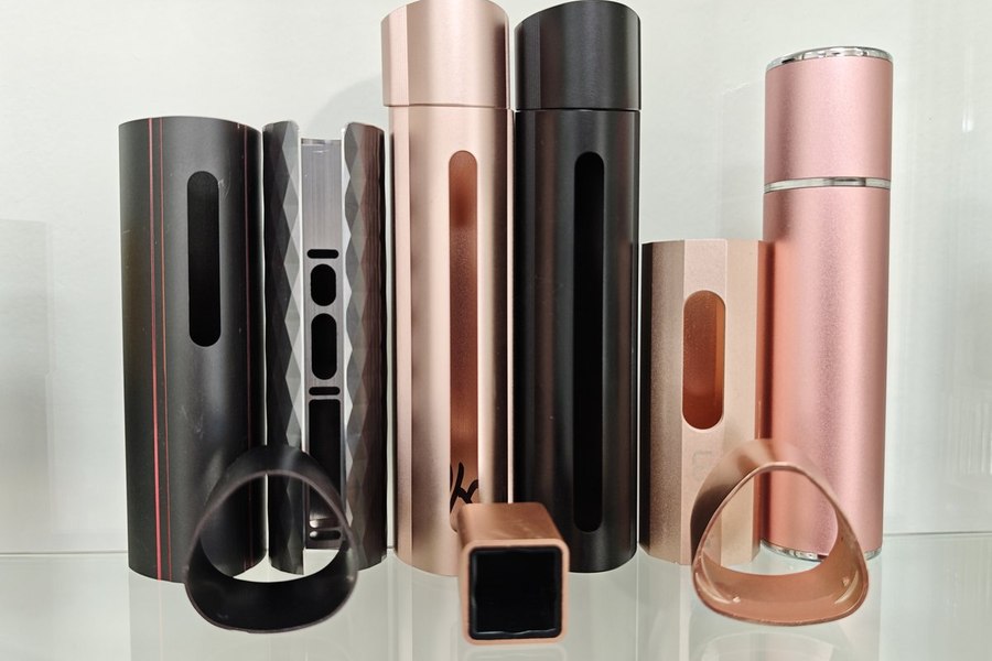
Medical & Beauty Device Enclosures
Cosmetic-grade aluminium housings for beauty instruments, hair styling tools and portable medical devices — polish-free 6063,…
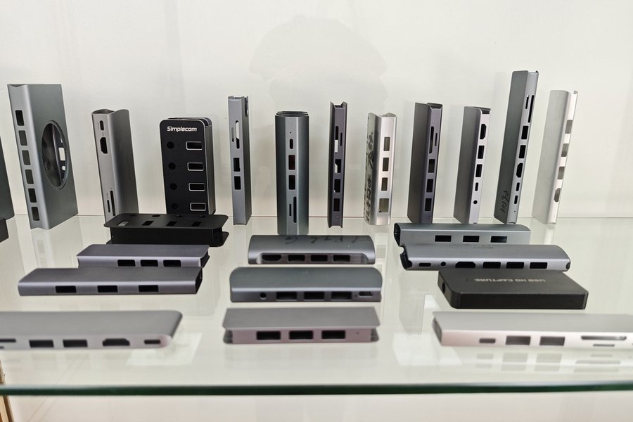
3C Consumer Electronics Enclosures
High-volume aluminium shells for external SSDs, docking stations, power banks and wireless chargers — ±0.005 mm cut-to-length…
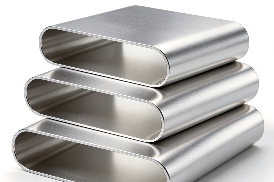
Industrial Control & Instrument Enclosures
Extruded aluminium housings for PLC controllers, HMI panels, sensors and test instruments — machined cut-outs, grounding…
Send your module drawing and shielding requirement — DFM feedback and a tooling quote within one working day.